A simple, easy to build and tune 14MHz SSB transceiver is described. I hope that this transceiver fulfills the need among Indian amateurs for a low-cost SSB transceiver that is easily built.
Linear Amp
I had the following objectives while designing this transceiver:
Easily procured
All the parts required for this set should be
universally available. This meant eliminating any low noise FETs, toroids,
special ICs, etc. It also meant using ladder filter made out of the most
commonly available microprocessor crystals.
Easy to build
The design should not have any critically tuned
parts, or too many settings to be played around with. This meant that the
amplifying stages should be of broad-band nature, with moderate gain controlled
with extensive feedback.
Low-cost
Almost any low power, plastic case NPN transistor with Ft
above 150 MHz can be used. I used BC547 (a local equivalent of BC107 and BC147)
although probably any transistor like the 2N2222 or 2N3904 will work. This is
because gain and impedances of each stage are controlled by the feedback
circuitry and not by any particular transistor's parameters.
Coils
Beginners always have a problem winding coils. They are also
a pesky source of radiation leaks and unwanted couplings. We have tried keeping
the coils to a minimum. Where required, I have used toroids created out of nylon
tap washers as coil formers. The tap washers cost about 50 paise each (about 1
cent).
Bi-directional
My previous experience with SSB transceivers
convinced me that using bi-directional circuitry is an elegant and simple way to
‘transceive’. The most important benefit is reuse of BFO, VFO, RF band pass and
crystal filters with minimal switching. Transmit/receive switching is
accomplished by a simple DPDT switch, eliminating the need for any elaborate T/R
mechanism.
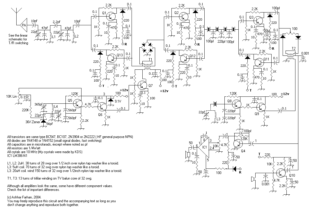
Each amplifier uses an RF feedback resistor and emitter degeneration to control gain as well as provide well defined input and output impedances. The relationship between the two is simple and very effective:
R-feedback * R-emitter = R-input * R-outputThus, if we choose a feedback of 1000 ohms and Emitter degeneration of 10 ohms, we can expect an input impedance of 50 ohms and output impedance of 200 ohms. This is illustrated as:
1000 * 10 = 10,000 = 50 * 200The gain is a little more complex to calculate, enough to say that in our case, the above values should yield a gain of about 16db throughout the HF spectrum. For a more detailed explanation, you can refer to the chapter 2 of Experimental Methods in RF Design, the new ARRL book on home brewing.
The simplest way of achieving bi-directional amplification is by strapping two such amplifiers back to back as is done in our design (we use three stages of bi-directional amplifiers as you can see in the circuit). By applying power to either of the two back to back amplifiers we can control the direction of amplification.
Even though only one of the two amplifiers is powered on at any time, the inactive amplifiers circuitry still affects the active amplifier. If you closely look at any of the pairs in the circuit, you will see that the feedback resistor between the base and collector of each stage is coupled through the input/output capacitors to the feedback resistor of the other transistor of the pair. Thus, for each stage, the RF feedback consists of two resistors in parallel (each 2.2K resistor, effectively providing a total feedback resistance of 1.1K in each direction). Accordingly, in the above design, we have increased each feedback resistor to 2.2K instead of the nominal 1K calculated above.
The amplifiers have resistive load. This reduces the signal handling capability of the stage but they provide an excellent and very stable output termination. The resistive load (of 220 ohms in our case) of the inactive stage will appear to load the active stage’s input but for the diode in series with the load. The diode serves to isolate the inactive amp’s load from the input of the active stage.
An interesting tidbit is the amplifier that follows the crystal filter during receive is capable of even amplifying audio noise. Thus, it has to be bypassed for audio as well as radio frequencies. We used a 100pf output coupling instead of the usual 0.1uF to provide roll-off for audio frequencies.
A Hartley FET is almost a norm in VFO designs. Cost and FET availability constraints forced us to use bipolars instead design. It takes about 5 minutes for the VFO to stabilize after applying power. There is a lack of proper measuring equipment in the home lab, thus no attempt was made at measuring the phase noise of the VFO. It is assumed to acceptably low from experiencing the sharp tuning of receiver and nearly 20 volts of RF across the inductor.
Buy about 10 crystals. Assemble the BFO circuit, solder in each crystal and note the exact frequency in a receiver or a frequency counter coupled to the output of Q9. Use four crystals with the closest match for the filter.
A distilled down version of the design process of the ladder is available at this site on http://farhan.net.co.nr/xcvr1.html. In my correspondence with W7ZOI, he has pointed out that my measured motional parameters for the crystals are not common (I measured a 5 KHz shift using the G3UUR’s circuit). I would suggest that you buy only those crystals marked KDS (I guess they are a Chinese/Asian import). They cost about Rs.10 each in the local marked (25c).
Component values given for the BFO and the SSB filter have worked well for a number of hams in India who have duplicated the circuit. What follows is a discussion for those who wish to change them.
You can use the values provided in the circuit as a starting point. If you find the bandwidth too narrow, then decrease the capacitances and if you find the bandwidth wide, then increase the capacitances. Maintain the ratio of capacitances as given in the circuit.
Beginners should note that improper setting of the BFO can sometimes lead you to thinking that the bandwidth is narrow. Be sure that the BFO is at the lower edge of your filters skirt. The easy way to achieve this is tune up the band until you start hearing a strong carrier. It should start out shrill like cat’s voice and as you tune towards it, the pitch should drop to low rumble and then vanish. If it peaks up again after dropping to the rumble, then the BFO is sitting in the middle of the filter pass-band. In our case, you should add turns to the coil in series with the BFO crystal. On the other hand, if the signal drops out before it gets to the low rumble, then the BFO is too far below the filter’s center frequency and you need to take out some turns from the coil.
If you want to use this design with lower sideband, the BFO crystal will have to be set to the upper edge of the filter pass band. To do that, substitute the coil with a 22pf trimmer as shown in the dotted figure in the circuit.
A double tuned filter precedes Q1 as the RF amplifier. The RF amplifier establishes a proper broadband termination for the RF filter as well as the diode ring mixer. We use a singly balanced mixer to keep the construction challenge a minimum. It is fed by a broad-band amplifier that is fed by the VFO. The transformer used in the mixer is wound on a TV balun core.
The Q2, as a post mixer amplifier provides a proper termination for the mixer as well as the crystal filter that follows.
The Q3 IF amplifier has two interesting diversions. It was noticed that the IF amplifier is capable of working perfectly from audio frequencies up into lower VHF. It needs power line bypass in at audio frequencies as well HF. Hence, you will see the 50u capacitor on the collector load of Q3. The output of the IF amplifier is coupled to the second mixer (acting as a product detector) through a 100pf. This was done to eliminate audio response of the IF from getting into the mixer.
The audio amplifier is straightforward and it is capable of feeding a small speaker. Incidentally, highest gain in the circuit is provided by the audio preamplifier. A low cost audio power amplifier is based on LM386-N1. A warning, the LM386 comes in a number of versions, be sure to buy the N1. The rest may not work with the given power supply.
The microphone amplifier based on Q10 has a direct coupling between the base and the microphone. This was done as the electret microphones that are built into the PC headsets need 5V bias. If your microphone does not need the bias, solder a 1uF between the microphone and the base of Q10.
The modulator needed a 10pf strapped to one of the two diodes for nulling the carrier. You will have to play with soldering it to either side or leaving the 10pf out completely.
The exciter uses the same line up as the receiver. The SSB output across a 50 ohms load connected to the RF filter is about 150mV peak-to-peak.
The pre-driver is built onto the main board of the transceiver and away from the linear amplifier board for reasons of stability.
Each amplification stage shifts the phase of the signal by 180 degrees. The low-pass filter in the transmitter output will shift the phase by another 180 degrees. Thus, the total phase shift in three stages plus the LPF will be 0 degrees, nearly ripe conditions for self oscillations.
Instead, we chose keep the pre-driver close to the RF band pass filter so that any stray pick by the link from the pre-driver to the linear board will only be a negative feedback (180 degrees out of phase). The additional benefit is that the signal level is much higher at the output of the pre-driver.
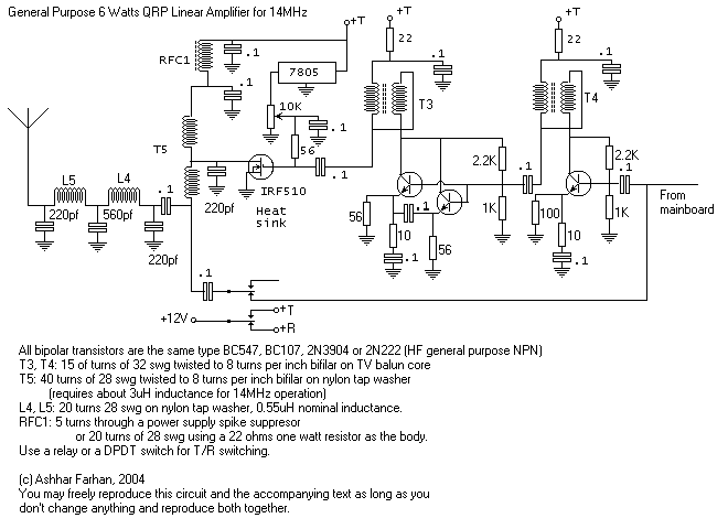
For the driver stage, we used two general purpose npn transistors in parallel for higher current handling. Each has a separate emitter resistor though both share the same emitter degeneration. This setup saves cost of a more expensive driver transistor. The driver uses another TV balun core as a wide-band transformer.
The PA transistor is a power MOSFET - the IRF510. It is no longer manufactured by International Rectifiers. It is now manufactured by Samsung Electronics Company. To eliminate the need for a toroid core, the nylon washer as tried as a broadband output transformer. It uses 40 turns of bifilar winding. These many turns surely lead up to self capacitance within the coil. In this circuit, the self capacitance is absorbed in the low pass filter’s capacitors and it forms a part of the LPF circuitry. Thus, the need for a costly and hard to find broadband core was eliminated. This design can only be applied where the low pass filter directly follows the output transformer.
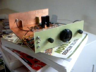
The entire exciter is built on single 8 inches by 2-1/2 inches strip of single side copper clad board. You can also use a thin copper sheet instead.
Start from the audio end and end at the RF end. Don’t skip on doing just the receiver first or the transmitter portions alone. If you do, you might be stuck without much space to wire the remaining portions and the circuit will not perform well either as some feedback components are shared between the two.
The layout is really not very critical. Broadly follow my lineup and you will not go wrong.
I made a mistake of placing the VFO on the main board and away from the tuning capacitor. This has made the VFO slightly microphonic. Keep the VFO on a separate board. Shield it if you want better stability. If you can, hunt around for a 56pf polystyrene capacitor for the VFO. They are a little hard to get in India these days. I bought a whole bag when I saw them at a radio spares shop last month. If you don’t get a polystyrene capacitor, then bite the bullet and use a regular disc ceramic. It will drift a little, so you will have to tune more often. In any case, the VFO runs at 4 MHz, so you don’t have to really make an effort at stability.
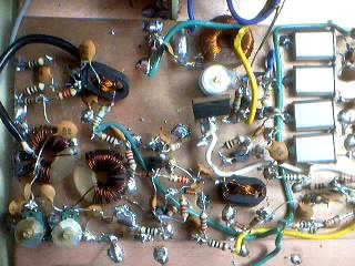
The broadband transformers used in the mixers are 15 turns of 32 swg trifilarly wound on TV baluns. The correct way to do this is to take twist 15 inches of three 32 swg together (you can tie one end to a fixed door handle and loop the other through a hook) until you have about 8 turns to an inch. You have to pass these around15 times through the balun core. See the pictures.
As an interesting note, in my previous design, I tried using BF195s and switched over the expensive 2N3866 because I found their gain quite low. I blamed this on spurious quality of the transistors in the market. I was wrong. The BF195 is designed to decrease gain with increasing current so that it can be used as an IF amplifier with forward AGC characteristic. My bad. My suggestion would be, avoid BF195. You can use BF194, 2N2222, 2N3904, BC109, BC107 and the rest. Don’t use transistors meant for VHF/UHF purpose, they tend to be unstable with even the slightest coupling and they are expensive.
I used an LM386N1 as the audio amplifier. Feel free to substitute. If the audio amplifier has enough gain to handle a direct microphone input, it is good enough.
I used TV baluns cores for broad-band transformers. You can try using FT37-43 toroids with 15 turns trifilarly on T1 and T2 and 15 turns bifilar on T4 and T4 with 32 swg wire, twisted to 8 turns per inch.
The linear chain was initially unstable. It tended to oscillate in the 14MHz band as well as around 500 KHz. I traced the 14MHz oscillations to a choke that I was using at the output of the balanced modulator. It has been removed. The 500 KHz oscillations were because of excessive gain in the driver and pre-driver stages. From 5 ohms, the emitter degeneration has been increased to 10 ohms and better bypassing on the power rail has eliminated the oscillations.
The receiver is as hot as I need it to be on 20 meters. Signals from USA, Europe, South Africa and of course India were heard with clarity reminiscent of a clean Direct-conversion receiver on the first evening. The transmitter is powerful enough for local rag chew and it is a modest challenge for DX. VU2PEP has an excellent two element beam at 20 meters at about 40 feet height. DX is easy for OM Paddy who uses the rig regularly. We netted LA2FKA within the first 20 minutes of firing up the rig.
No, I don't offer PCBs. I don't repair rigs. I don't offer kits. I might do a PCB for this rig (I hate PCBs, they hamper experimentation). If and when I do, I will put the template on this site. Don't ask me when.
This transceiver is dedicated to the memory of OM Juggie, SK (VU2JH) who was a great organizer of India hams, he wrote technical articles in Electronics For You magazine about amateur radio, spurring many to take on ham radio as a hobby. He organized the Millennium Ham Meet in the year 2000. He was always searching for a good and simple homebrew SSB transceiver. He died young. He gave me my first morse key.
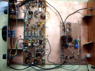
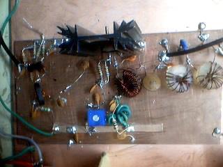
Front-end assembly
The coil
at the top is the VFO. Note that the regulator IC on the board is now replaced
in the schematic with a low cost Zener diode.
The two coils in the lower left
are the RF band pass filter. The RF amplifier, front-end mixer and the ladder
filer can be seen in the center
The top left has the linear pre-driver
stage
The lower
left corner is the post-mix amplifier (when receiving).
The upper left corner
is the IF amplifier (when receiving).
The upper center is the
detector-cum-modulator.
The upper right corner is the mic amplifier.
The
lower right corner is the receiver audio pre-amp and the LM386.
In the
center, you can see the BFO.