The experiment of the 10MHz receiver made with "MC3362P"(June 28, 1998) |
 The IC "MC3362P" of Motorola company is designed for narrow-band
FM double super receiver circuit. I thought that this IC was useful for
the production of the 10MHz CW transceiver. Then, I began an experiment. A
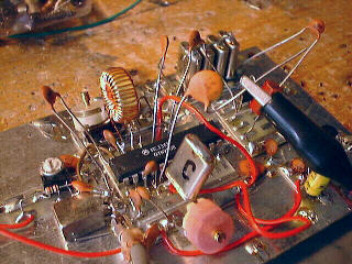
photograph is the test scenery. The IC "MC3362P" of Motorola company is designed for narrow-band
FM double super receiver circuit. I thought that this IC was useful for
the production of the 10MHz CW transceiver. Then, I began an experiment. A
photograph is the test scenery.
I tested this circuit referring to the article of the magazine "QST" issued in 91. The kit of the transceiver which is almost the same as the article is put on the market in the United States. The outline of the circuitIt is an input tuning circuit that it can be seen on the left end of the photograph. A signal is inputted to the 1stMIX circuit (double balanced mixer) inside the IC from here. Troidal-core of Amidon company and that next trimmer capacitor are connected with the first local oscilator inside the IC. Actual tuning operation is done by controlling a variable capacity diode inside the IC with the half-fixed resistor in that left. When it turns a half-fixed resistor, frequency changes in the range of 6.100`6.150MHz. The output of 1stMIX goes into 2ndMIX (DBM) inside the IC next time through 4 elements crystal filter (-3dBBW=1.0kHz) of 4.000MHz. BFO is composed of the crystal of 4.000MHz and the 2ndLO circuit inside the IC. The weak signal of -10dBuV can be received only by the IC.MC3362P gains the profit of 40dB only with two inside MIX circuits. The weak signal of -10dBuV from Standard Signal Generator could be received when a crystal earphone was connected with the output of 2ndMIX directly. A power supply uses 5V stabilized with 3 terminal regulator, and circuit current is 5mA. It is a saving energy type very much. Next, I wanted to add an AGC circuit. Therefore, I added two non-tunning amplifiers of 2SK241Y after the IF crystal filter. I connected the AF amplifier of LM386. Then, the very weak signal of -20dBuV from SSG became loud sound. When I connected an antenna, I could listen to the communication of the signal of FAX, RTTY and CW inside the band . The frequency of the inside VFO circuit is very stable.I was very much surprised that the frequency of VFO by the oscilator inside the IC was very stable in this experiment. When a troidal-core T-50-6 with 25 turns, a silvered mica capacitor of 100pF, a trimmer capacitor of Philips company of 100 pF and a variable capacity diode inside the IC were combined, a change in frequency, after 30-minute rest from the power supply injection, was within 100Hz. I can judge that this becomes utility fully. I turned on the power all night long, and left this on trial. A change in frequency until the next morning was about 1kHz. This has the influence of the room temperature, too. And, when the FCZ coil (This is the coil developed by JH1FCZ, Mr. Okubo, and this is known well in the Japanese ham.) was used for the coil of VFO, a change in frequency was big, and it wasn't practical. It is probably a cause that the congeniality of the temperature character was bad. The subject which should be examined from now on.Well, a future subject. I want to compose an AGC circuit by using the gate of 2SK241Y which put it after the crystal filter. I want to start the experiment of the transmitting part, too. I will mix each output of VFO and BFO with NE612. I will connect an amplification circuit by 2SK241 and 2SC1815 with the mixer. I will be able to complete the transmitting part of about output 100mW in this. How do you use the 2 pin of MC3362P?By the way, by the data seat of MC3362, it is being written in two LO circuits inside the IC that all the buffer amplifier output pins are set up. As for the 2nd LO, though the 2 pin is a buffer amplifier output pin, the way of using it isn't shown only with this pin as a circuit example mentioned in the data seat. By the inside equivalent circuit figure, because a fixed electric current circuit is set up in the emitter, a capacitor is only combined, and output is supposed to be able to be taken out. It thought like that, and I tried to connect a frequency counter with this pin. But, I couldn't measure frequency at all. I want to learn it about this thing if it has the knowledge which someone is familiar with. When I wrote it like that, JA9TTT/ 1, Mr.Kato explained to me as follows. 'The inside circuit is probably as the equivalent circuit being written in the data seat. But, as for this IC, it is very stingy with circuit current. The output impedance seems to be very higher though it is an emitter-follower circuit in the cause. If you apply this pin to something, you had better add the buffer amplifier of FET. Or, you may be good when you ignore the fixed inside electric current source and put the resistor of some k-ohm to the ground with the outside and currents are increased.' I connected an oscilloscope once again, and observed the state of the output of 2 pin. Then, I could confirm that the output of 150m Vp-p appeared certainly in 2 pin. I was doing carelessly. And, the voltage of the 1st LO buffer output is about 750m Vp-p. It is powerful. |
| The simple 7MHz CW transceiver made with Motrola MC3362P |