Andy's Technical Information Page
MC145106 MM55106 MM55116 MM55126 PLL Frequency Synthesizer
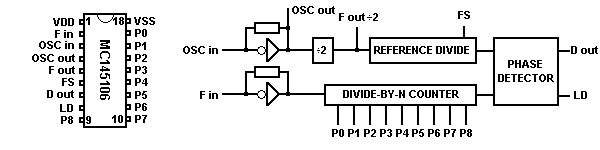
Overview
The MC145106 has circuitry for a 10.24 MHz oscillator or may operate with an external signal. The circuit provides a 5.12 MHz output signal, which can be used for frequency tripling. A 512 programmable divider divides the input signal frequency for channel selection. The inputs to the programmable divider are standard groundtosupply binary signals. Pulldown resistors on these inputs normally set these inputs to ground enabling these programmable inputs to be controlled from a mechanical switch or electronic circuitry.
The phase detector may control a VCO and yields a high level signal when input frequency is low, and a low level signal when input frequency is high. An outoflock signal is provided from the onchip lock detector with a ³0² level for the outoflock condition.
Single Power Supply
Wide Supply Range: 4.5 to 12 V
Provision for 10.24 MHz Crystal Oscillator
5.12 MHz Output
Programmable Division Binary Input Selects up to N=512
OnChip PullDown Resistors on Programmable Divider Inputs
Selectable Reference Divider, 1024 or 2048 (Including ÷ 2)
ThreeState Phase Detector
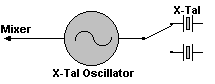
Down-converting of the frequency to the divider
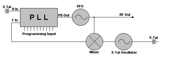
The X-Tal frequency is f XTAL = f OUT - f IN
| The output frequency can be changed by changing the mixing-xtal or add a new mixing-xtal to the oscillator. |
 |
| Pin | Name | Description |
|---|---|---|
| 1 | VDD | Positive Power Supply |
| 2 | F in | Frequency input to programmable divider - Max. 3MHz |
| 3 | OSC in | Oscillator input |
| 4 | OSC out | Oscillator output |
| 5 | F out | Reference OSC frequency divide by 2 output |
| 6 | FS | Reference Oscillator Frequency Division Select. 1=10 kHz, 0=5 kHz |
| 7 | D out | Detector output (for control of external VCO) |
| 8 | LD | Lock Detector |
| 9 | P8 | Programmable inputs (Binary) |
| 10 | P7 | Programmable inputs (Binary) |
| 11 | P6 | Programmable inputs (Binary) |
| 12 | P5 | Programmable inputs (Binary) |
| 13 | P4 | Programmable inputs (Binary) |
| 14 | P3 | Programmable inputs (Binary) |
| 15 | P2 | Programmable inputs (Binary) |
| 16 | P1 | Programmable inputs (Binary) |
| 17 | P0 | Programmable inputs (Binary) |
| 18 | VSS | Ground |
| P8 | P7 | P6 | P5 | P4 | P3 | P2 | P1 | P0 | Divide by N |
|---|---|---|---|---|---|---|---|---|---|
| 0 | 0 | 0 | 0 | 0 | 0 | 0 | 0 | 0 | 2 |
| 0 | 0 | 0 | 0 | 0 | 0 | 0 | 0 | 1 | 3 |
| 0 | 0 | 0 | 0 | 0 | 0 | 0 | 1 | 0 | 2 |
| 0 | 0 | 0 | 0 | 0 | 0 | 0 | 1 | 1 | 3 |
| 0 | 0 | 0 | 0 | 0 | 0 | 1 | 0 | 0 | 4 |
| 0 | 0 | 0 | 0 | 0 | 0 | 1 | 0 | 1 | 5 |
| 0 | 0 | 0 | 0 | 0 | 0 | 1 | 1 | 0 | 6 |
| 0 | 0 | 0 | 0 | 0 | 0 | 1 | 1 | 1 | 7 |
| 0 | 0 | 0 | 0 | 0 | 1 | 0 | 0 | 0 | 8 |
| - | - | - | - | - | - | - | - | - | - |
| - | - | - | - | - | - | - | - | - | - |
| 0 | 1 | 1 | 1 | 1 | 1 | 1 | 1 | 1 | 255 |
